Optical Crosstalk in CMOS Image Sensors
Chris Fesenmaier and Benjamin Sheahan
Psych 221 - Winter 2006-2007
| Welcome | ||
| Introduction | ||
| Methods | ||
| Pixel Scaling | ||
| Methods | ||
| Results | ||
| Conclusions | ||
| References | ||
| Crosstalk Reduction | ||
| Methods | ||
| Air Gaps | ||
| Light Guide | ||
| Metal Mirrors | ||
| Results | ||
| Reference | ||
| Air Gaps | ||
| Light Guide | ||
| Metal Mirrors | ||
| Conclusions | ||
| References | ||
| Appendices | ||
Pixel Scaling - Methods
Methods
To investigate the impact of pixel scaling on the quality of the image the scaled pixels were simulated using the OptiFDTD maxwell electromagnetic field solver simulator.
The particular focus of this work is to investigate the optical path from the surface of the image sensor to the silicon photo diode as the pixel pitch is decreased from 2.2µm to 1.45µm and then to 0.97µm.
The metrics which were used to evaluate the quality of the optical pathway were optical power received by the photo diode and the spectral and spatial (optical) crosstalk to adjacent pixels. The effectiveness of the micro lens was evaluated by comparing the optical power in the center of the pixel region. A fill factor of 50% was assumed.
Description of the optical path and the simulated structure
The optical path comprises of the micro lens, the silicon nitride passivation, the color filter, array, the silicon dioxide interlevel dielectric, boron phosphate silicon glass and silicon dioxide and finally the silicon photo-diode sensor.
A 2 dimensional periodic two pixel structure was used to model the pixel array. The pixel on the left is the desired pixel and has a Blue, Green or Red color filter. The pixel on the right has a black color filter (Ideal Absorbing Filter). Any optical power which appears at the photodiode on the right is spatial (Optical) Crosstalk The boundary conditions were configured so that the left edge wraps around to the right edge and all the crosstalk optical is accounted for.
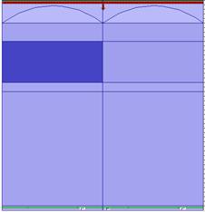
Figure 2: 2.2um Pixel Layout
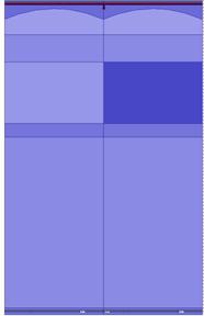
Figure 3: 1.45um Pixel layout
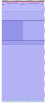
Figure 4: 0.97 um Pixel Layout
Micro Lens Design
The radius of the micro lens was simulated over a range of 1.51µm to 4.33µm to investigate the impact of the depth of focus on the optical power received by the pixel photo diode. The effectiveness of the micro lens was determined by integrating the optical power received in the central region (50% Fill factor) of the pixel and comparing it to the power received in the entire pixel.
The micro lens focal length is calculated using [3]
n1/s + n3/ s' = n3/f
where
n1 = 1.000 Refractive index of Air.
s = infinity Distance to Object.
n3 = 1.47 Refractive Index of Silicon Dioxide between the micro lens and the photodiode.
f = Focal length from the micro lens to the photodiode.
s' = 4.1µm Stack height.
The object to be focused is at infinity compared to the dimensions of the micro lens thus the focal length is equal to the stack height:
f = s' = 4.1µm.
The "lens maker's equation" was used to calculate the radius of the micro lens
![]()
where
n1 = 1.00 Refractive index of Air
n2 = 1.636 Refractive index of the micro lens
n3 = 1.47 Refractive index of silicon dioxide stack
r1 = Desired Radius of the top surface of the Micro lens
r2 = infinity Flat bottom surface.
The thickness of the micro lens is calculated by solving for thickness using the following equation:

![]()
The calculated value of the Micro lens radius was 1.77µm and the thickness was 0.38µm.
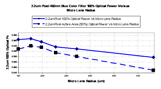
Figure 5: Received Optical Power versus Micro Lens Radius for a 2.2 µm Pixel at 450nm and a Blue Color Filter
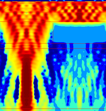
Figure 6: Energy Flow (Poynthing) Lens radius of 1.77um and thickness of 0.38um