Optical Crosstalk in CMOS Image Sensors
Chris Fesenmaier and Benjamin Sheahan
Psych 221 - Winter 2006-2007
| Welcome | ||
| Introduction | ||
| Methods | ||
| Pixel Scaling | ||
| Methods | ||
| Results | ||
| Conclusions | ||
| References | ||
| Crosstalk Reduction | ||
| Methods | ||
| Air Gaps | ||
| Light Guide | ||
| Metal Mirrors | ||
| Results | ||
| Reference | ||
| Air Gaps | ||
| Light Guide | ||
| Metal Mirrors | ||
| Conclusions | ||
| References | ||
| Appendices | ||
Introduction
CMOS Image sensors dominate the mobile phone camera market. The replacement of the charge coupled device (CCD) by the CMOS imager was made possible by the Moore's Law Scaling of the CMOS processes and devices. This scaling enabled the CMOS imager to improve in quality to compete with CCD Imagers in low cost mobile and high volume digital still camera and video applications.
Why have CMOS imagers replaced CCD Image Sensors?
The economic advantage is that the CMOS imagers can be built in a CMOS semiconductor fabrication factory which was previously used to manufacture dynamic random access (DRAM) memories or CMOS products.
Moore's laws scaling has enabled a larger number of pixels to be fabricated in the same silicon area which means costs are similar or lower. This process and device scaling has the increased spatial resolution of the CMOS image sensors. The cost is dominated by the area of the imager and the wafer. The CMOS imagers use mainstream and depreciated semiconductor fabrication equipment and factories. However the CCD imagers use relatively high voltages to deplete the silicon and thus define the pixel. The high voltage processes are no longer standard and the CCD fabrication is not main-stream and does not benefit from the enormous investment in scaling that has been expended on mainstream CMOS devices and semiconductor process equipment. Thus, CCD semiconductor equipment and factories are dedicated to imager production only so that the return on investment is relatively poorer than that for a CMOS imager built on an aggressively scaled and depreciated CMOS fabrication facility.
What are the limits of CMOS scaling applied to the CMOS imager?
The CMOS imager replaced the CCD imager by scaling to a lower cost and higher performance.
The reasons for the continued scaling the CMOS imager are as follows:
• Increase customers perceived value by increased number of pixels.
• Reduce Cost
• Survive by continued innovation.
• Crush competitors by rendering their products obsolete.
• Increase Imager spatial resolution.
This strategy is the reason why the CMOS imager has been extraordinarily successful in displacing CCD from low cost and high volume applications.
The present state of the art CMOS image sensor has 6.4 million pixels and has a pixel size of 2.5um x 2.5um[1] from Sony or 7.2 million pixels and a pixel size of 2.25um x 2.25um[2] from Samsung.
The scaling road map for CMOS imagers is shown in figure 1.
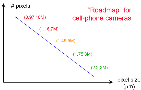
Figure 1
Optical design of scaled image sensors