Optical Crosstalk in CMOS Image Sensors
Chris Fesenmaier and Benjamin Sheahan
Psych 221 - Winter 2006-2007
| Welcome | ||
| Introduction | ||
| Methods | ||
| Pixel Scaling | ||
| Methods | ||
| Results | ||
| Conclusions | ||
| References | ||
| Crosstalk Reduction | ||
| Methods | ||
| Air Gaps | ||
| Light Guide | ||
| Metal Mirrors | ||
| Results | ||
| Reference | ||
| Air Gaps | ||
| Light Guide | ||
| Metal Mirrors | ||
| Conclusions | ||
| References | ||
| Appendices | ||
Methods
Finite-Difference Time-Domain (FDTD) Simulation
To simulate the propagation of light inside the image sensor, we used Finite-Difference Time-Domain (FDTD) simulation. FDTD is well-suited for simulation of the behavior of light on a sub-wavelength scale, a regime where diffraction and other complex phenomena dominate. Given a layout, material parameters (refractive index), and a light source, this technique explicitly solves Maxwell's equations for electric and magnetic fields at finely spaced (~10 nm) grid points. It then moves forward in time by a very small amount (~10^-17 sec, about the time it takes light to travel a few nanometers) and solves the equations again using the previously solved values.
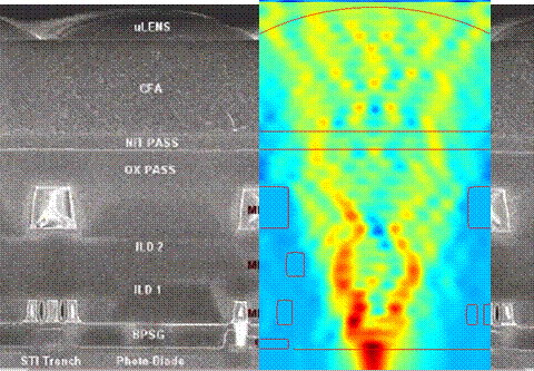
After a number of time steps deemed sufficient for convergence to a steady-state solution, the energy flow, known as the Poynting vector, is computed and displayed as in Figure 2. In addition, the power flux falling on an arbitrary surface, such as the active pixel area, is calculated. The construction of the FDTD layouts and display of the Poynting vector with the pixel structure outlined was facilitated by Matlab scripts that Chris had written in the course of his research assistantship.
|
Fig. 2. A sample FDTD result, showing the magnitude of the Poynting vector in the vertical direction as a function of position in the pixel. The pixel layout was adapted from the scanning electron microscopy (SEM) image from Rhodes [1]. |
FDTD Pixel Simulation
The specific software package that we used, OptiFDTD, is capable of full three-dimensional simulation, but processing time restricted our work to two dimensions. The particular type of FDTD simulation we used was continuous wave, meaning that only one wavelength of light is used. Since each simulation was at a specific wavelength, we restricted our work to three wavelengths representative of the color filters in a CMOS image sensor: 450 nm (blue), 555 nm (green), and 650 nm (red). This also means that we only needed to know the materials' characteristics at these wavelengths, although we sacrifice knowledge about the behavior of the image sensor at the in-between wavelengths. We obtained refractive index data for some materials from Palik [2] and made approximations for others.
Since we worked in two dimensions, the simulations are a cross-sectional approximation of an actual pixel. Given that we are modeling a finite area, it is important to define the simulation behavior at the edges of the domain. In the direction parallel to the image sensor plane, we used periodic boundary conditions that would effectively "wrap around" any electromagnetic wave to the other side. In the direction normal to the image sensor plane, we set absorbing boundary conditions so that light that was incident on these edges would leave the domain.
Even with a robust simulation tool, the evaluation of crosstalk is not straightforward because it is impossible to separate the light that is intended for one pixel from the light intended for another pixel. While it is simple to restrict the incoming light to the width of a single pixel, the wave will quickly spread out due to diffraction. As a result of tests done by Chris during his research assistantship, it was decided that strongly absorbing "black" color filters would be used as the color filter of the neighboring pixel. While diffraction would still occur after the color filters, it would be less drastic and take place further down the optical path, reducing its influence.
Pixel Structure
The pixel structures were made to be generic representations of current examples in literature. Although the structure has been significantly simplified, the overall optical characteristics of the pixel are the same. The pixel, as laid out in OptiFDTD, is shown in Figure 3 and described below.
|
Fig. 3. Two-pixel structure as defined in OptiFDTD. Note the different shades of the color filters of the pixels. |
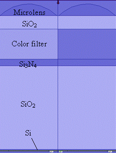
The light first travels through air (n = 1) and enters a spherical microlens of refractive index ~ 1.6. Below the lens is a silicon dioxide (n ~ 1.46) layer that acts as a passivation layer. Next is the color filter layer that varied according to the simulation, although for simplicity, it is always the same thickness. Below this is a silicon nitride (n ~ 2.0) passivation layer, followed by the thick silicon dioxide interlayer dielectric (ILD). This layer would normally contain several layers of metal interconnects, but they were omitted due to wide variations in metal layouts among designs, as well as their unpredictable electromagnetic effects. At the bottom of the pixel is the silicon (n ~ 4.0) substrate where the incident light is converted into electrical current.
To more precisely reproduce the characteristics of a real CMOS image sensor, where pixel circuitry often occupies a significant portion of the pixel space, we limited the light collecting area of the silicon substrate. This is represented by the fill factor of a design, which is the fraction of the pixel area dedicated to collecting light.