Optical Crosstalk in CMOS Image Sensors
Chris Fesenmaier and Benjamin Sheahan
Psych 221 - Winter 2006-2007
| Welcome | ||
| Introduction | ||
| Methods | ||
| Pixel Scaling | ||
| Methods | ||
| Results | ||
| Conclusions | ||
| References | ||
| Crosstalk Reduction | ||
| Methods | ||
| Air Gaps | ||
| Light Guide | ||
| Metal Mirrors | ||
| Results | ||
| Reference | ||
| Air Gaps | ||
| Light Guide | ||
| Metal Mirrors | ||
| Conclusions | ||
| References | ||
| Appendices | ||
Crosstalk Reduction - Methods
For simulations of the crosstalk reduction methods, the 1.75 µm pixel pitch was chosen as a technology node when optical crosstalk limits the performance of the sensor and the proposed methods may first be implemented. To limit the number of simulations necessary, all tests were at 650 nm (red) light. It was expected that this part of the visual spectrum would have the worst crosstalk problems due to increased diffraction at longer wavelengths. The active (light-collecting) portion of the silicon substrate was limited to the center 1.2 µm of the pixel, a fill factor of 47%. To provide parity between each light guiding design, the space above the remaining 0.55 µm was reserved for metal interconnects, although they were not included in the design for reasons discussed earlier.
For simulations where light enters normal to the image sensor, a two-pixel layout was used, one pixel with a red filter, the other black. Taking the periodic boundary conditions into account, this mimics a structure of an infinite line of alternating red and black pixels. Unfortunately, two-pixel simulations for angled incidence were not satisfactory due to the non-ideal behavior of the periodic boundary conditions for off-axis light. For this reason, simulations of off-axis incidence were done using a four-pixel periodic structure and the results for each pixel type (intended or unintended light recipient) represent the average value of the two pixels. Previous simulations have shown that the results for on-axis two- and four-pixel simulations are nearly identical, so the comparison between the two is sound. In the interest of time, the two-pixel on-axis simulations were performed with 5 nm grid spacing, while the four-pixel off-axis simulations used 10 nm grid spacing.
For off-axis simulations it was necessary to laterally shift the microlenses and color filters to guide the light onto the correct photodiode. This is done in real image sensors as well. The optimal shift was approximated through several trials and kept constant for all the light guiding simulations, except for the reference pixel, which required a larger shift.
A total of six different pixel designs (including a baseline reference design) were simulated at three angles (0, 15, and 25 degrees) to observe the performance of the crosstalk prevention methods. In the following sections, we will give a short overview of total internal reflection (TIR) and its implications for these designs, discuss each design individually, and then follow with a performance comparison between the techniques.
Total Internal Reflection
In order to understand how two of these techniques function, it is necessary to mention total internal reflection. When light is incident on a material interface, it is refracted at an angle according to Snell's law:
|
(1) |
When going from a high refractive index material to a lower one, there is an angle above which the light is reflected instead of refracted; this is called the critical angle. Using simple geometry, we can calculate the expression for the incident angle below which light will undergo TIR (here defined as the angle measured from the normal of the image sensor plane) as
|
|
(2) |

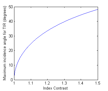
According to this equation, plotted in Figure 4, a higher index contrast (defined as ![]() so it is always greater than one when TIR is possible) yields a higher maximum incidence angle for TIR, which we would like to make as high as possible. This equation is very sensitive to even a small index contrast, as shown by the sharp rise in TIR angle as the index contrast increases.
so it is always greater than one when TIR is possible) yields a higher maximum incidence angle for TIR, which we would like to make as high as possible. This equation is very sensitive to even a small index contrast, as shown by the sharp rise in TIR angle as the index contrast increases.
|
Fig. 4. Relationship between the maximum angle of incidence for which TIR occurs and the index contrast. |