Methods: Simulation and Validation
Simulating a Pixel on MATLAB
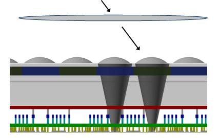
The MATLAB scripts used for the optimization calculations come to us courtesy of Dr. Peter Catrysse. The main script models a 2D cross-section of a pixel with a width of 3.3 μm and height 4.9 μm (not including the microlens height). Light incident on the pixel was represented as a lens illumination rather than a plane wave, and therefore modeled as a cone of light defined by its wavelength (we used 555 nm) and span angle. The microlens, located at the top of the pixel, serves to focus incident light down to the photodiode on the pixel floor, and is modeled in the script as an obstacle with a given curvature, refractive index, and width.
Light then propagates through the oxide, again specified by a given refractive index, and encounters the three metal wire layers (each with the same refractive index) modeled as infinitely long, infinitely thin 1D obstacles separated by a gap or aperture of given width. The adjustable parameters are determined by the structural limitations of the pixel itself, and were therefore restricted in this model to changing width and shift of the wire apertures along the x-axis.
The MATLAB code executes the propagation of light by using the input parameters of wire shift and location, as well as the given values of pixel dimensions and material properties, to calculate a new angular spectrum and amplitude of complex field of the incident light. The new values of angular spectrum and amplitude, calculated after each subsequent propagation, describes how the wave front has been modified after passing through the designated obstacle. Power is then calculated from angular spectrum and amplitude.
What Makes a Good Pixel?
Determining the relative improvements in light collection provided by various wire arrangements requires quantification of pixel efficiency. This model measures pixel efficiency by examining two different ratios. The overall power ratio compares the amount of light entering the pixel, measured just after propagation through the microlens, to the intensity of the light incident on the photodiode located at the pixel floor. Since it describes the amount of light both reaching the bottom of the photodiode and the amount lost over the course of the path through the pixel (quantities which are dependent on wire placement) this power ratio can serve as the cost function: light loss and light incident on the photodiode are maximized at the minimum value of negative overall power. The cost function assumes that the photodiode, whose width is half that of the microlens, is positioned at the location which maximizes light incident on it. This optimization step is already incorporated in the code.
The collected power ratio compares the intensity of light incident on the photodiode to the intensity of light falling on the pixel floor outside the photodiode. This ratio therefore describes the efficacy of the wire arrangement in focusing the path of light down to the photodiode. Tracking collected power ratio enables a qualitative assessment of crosstalk, which occurs when light falls outside the pixel floor and is incident on photodiodes of neighboring pixels. Crosstalk increases noise and reduced image quality; it is therefore a valuable quantity to keep in mind, and attempt to minimize, when considering the optimal pixel structure.
Optimization
To perform our optimizations we used the MATLAB function fminsearch. This function takes a function and a starting value and returns a local minimum of that function near the starting value. For our purposes we wanted to define a cost function and use fminsearch to find the pixel configuration with the minimum cost. Our goal was to maximize the overall power ratio at the photodiode compared to the initial light after the microlens. Therefore, our cost was defined as the negative of the overall power ratio, so that we could minimize it. The parameters that we examined were the aperture gap in each metal layer, and the horizontal shift of each metal layer.
Testing our Model: FDTD Validation
MATLAB offered a platform to rapidly perform the repetitive simulations necessary for optimization. But how accurate would the results of our simulations be? Were we making any approximations that would significantly affect our simulations? To test our model and validate our assumptions, we used a software package called OptiFDTD.
OptiFDTD uses the Finite-Difference Time-Domain (FDTD) method to simulate the behavior of light and other electromagnetic phenomena. An FDTD simulator divides a region of interest into a fine grid of squares (in the two-dimensional case) or cubes (in three dimensions). It then numerically calculates Maxwell’s equations, which describe the behavior of electric and magnetic fields, across the grid over finite increments of time.
The FDTD method is extremely powerful: a user can draw a region of interest, such as a pixel, and then numerically solve electromagnetic behavior that might be difficult to predict analytically. Unfortunately, however, FDTD is also extremely slow. Therefore, though it was a good way to validate our MATLAB results, it would have been a poor substitute for MATLAB in repetitive optimization experiments.
We planned to address two points of concern with OptiFDTD simulations. First, we wanted to make sure our physics engine was robust. A simulation of a particular pixel setup should produce identical results on MATLAB and OptiFDTD. Next, we wanted to test whether approximating wires as one-dimensional conductors was reasonable. In the MATLAB code, wires are assumed to be infinitesimally thin conductors that effectively form an ‘aperture’ for light to pass through. If this assumption is reasonable, a simulation of a pixel with wires of finite thickness and negligible thickness should produce similar results.
Validation of the Physics Engine
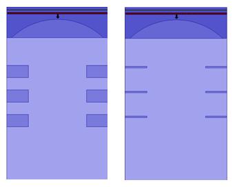
To test Dr. Catrysse’s MATLAB algorithm, we created a ‘blank pixel’, one devoid of any conducting wires, on both MATLAB and OptiFDTD. Light would enter this pixel through the microlens and propagate freely through the oxide layer. To simulate the operation of a photodiode, we would measure the intensity pattern of the light after it propagated 4.8μm—the distance from the microlens to the pixel floor. An OptiFDTD layout of this pixel setup is shown on the right.
The results of the experiment were better than we expected. Both simulations produced identical results, as the graphs below illustrate. The similarity between our frequency-domain simulation and OptiFDTD’s time-domain simulation suggest that the MATLAB physics engine was sufficiently robust for our optimization experiments.
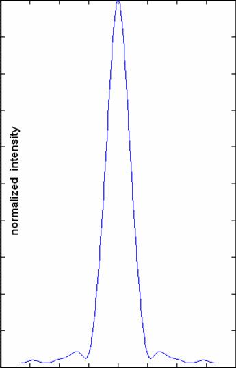
![]()
Left: OptiFDTD results; Right: MATLAB results.
Validation of the Wire Thickness Approximation
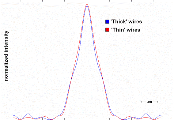
Since it was not possible to assign a thickness to wires in the MATLAB code, our test of the wire thickness approximation had to occur entirely in OptiFDTD. We created two pixel setups: one with ‘thick’ wires that measured 0.4 μm in thickness, and one with ‘thin’ wires that measured only 0.05 μm in thickness. If approximating wires as one-dimensional conductors was reasonable, then the ‘thin’ and ‘thick’ wire setups in OptiFDTD should produce almost identical intensity patterns at a depth of 4.8μm from the bottom surface of the microlens.
The results were as we expected. As the graph below illustrates, pixels with ‘thin’ wires and ‘thick’ wires behave almost identically under on-axis propagation. Though there is a slight difference in the intensity pattern produced by our approximation, the difference is more of shape than of magnitude, and is negligible for the purposes of our optimization experiment.
However, the on-axis results brought us to a new point of concern. From the simulation visualizations, we realized that our ‘thin’ wire approximation might behave differently from a ‘thick’ wire pixel in the off-axis case, or when light was incident at an angle. As the figure on the right illustrates, in the ‘thin’ wire approximation light can more easily propagate in the horizontal direction ‘under’ the wires. This could result in less guiding of incoming light or in other unexpected behavior.
To make sure that the ‘thin’ wire approximation was safe in the off-axis case, we tested the ‘thick’ wire and ‘thin’ wire pixels with light incident at 10 degrees. The results in this case were not similar. As the graphs below suggest, there were possibly significant differences in the intensity pattern at the pixel floor. But would this difference in intensity pattern affect the amount of light collected by the photodetector?
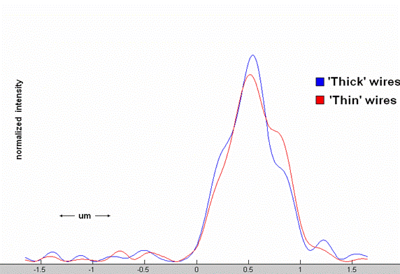
To find out, we simulated the light collection of the photodetector by integrating each intensity pattern across the location of the photodetector suggested by our optimization functions. We found a difference in the results. Though the ‘thin’ wire approximation indicated that we would collect 92.77% of the light that hit the pixel floor, once the thickness of wires was taken into account, this value dropped to 90.52%. This difference of 2.25% in the amount of light collected appears small, but is significant if we are trying to compare pixel designs that have similar light collection ratios. The uncertainty created by our ‘thin’ wire approximation is not enormous, but is still something that we had to keep in mind as we analyzed the rest of our results.
 Pixels in an image sensor receive light at different angles.
  FDTD simulators divide the region of interest into a grid and calculate Maxwell's equations over small increments of time.
 ![]()