Introduction and Background
A pixel in a digital image is a single sample of visual information. In a digital camera, however, a pixel is a small, complex structure designed to capture light and transmit samples of visual information. Inside a camera, millions of pixels are lined up in an array to form an image sensor.
Image sensors in most consumer digital cameras today use CMOS technology, the same technology used for most integrated circuits. Due to the process in which CMOS image sensors are fabricated, the wires that transmit information from pixels are located in layers above the individual photodetectors that collect incoming light (see ‘The Anatomy of a Pixel’). Fortunately, pixels are usually large enough to ensure that these wires do not block light from entering the photodetectors at the pixel floor.
As cameras get smaller, pixels must also, and the presence of wires becomes a problem. Wires can block light, especially light incident at an angle, from reaching the photodetector. How can we reduce the size of pixels while retaining their functionality? Specifically, where in a pixel should wires be placed to optimize the efficiency of light collection? In this project, we tried to address these questions by using simulations to investigate the effect of pixel wires on light collection.
The Anatomy of a Pixel
Every pixel in a CMOS image sensor has the same basic components: a microlens, metal wires, insulating oxide, and a light-sensitive photodiode. Light enters each pixel through the microlens, which measures a few microns in diameter. The lens focuses incoming light onto the photodiode. However, the path between the microlens and the photodiode is not empty. Due to the constraints of CMOS technology—specifically, the fact that semiconductor devices such as the photodiode can only be located on the pixel’s silicon substrate—wires that carry information from pixels must be placed above the photodetector. Therefore there are several layers of metal wires and insulating oxide between the microlens and the photodetector, and light must propagate between wires and through layers of oxide to reach the pixel floor.
Reducing Pixel Size: Problems
As imaging devices get smaller, pixel sizes must be reduced. However, reducing pixel size usually involves reducing a pixel’s cross-sectional area and increasing its stack height. This process of scaling pixels down presents two main problems. As the cross-sectional area of pixels decreases, so does the spacing between wires through which light must pass. As stack height increases, the required focal length of the microlens must increase as well. Therefore light that approaches a pixel at an angle is more likely to be blocked by wires. Since pixels throughout an image sensor receive light at different angles, wire placement must be optimized separately for pixels in different parts of the sensor.
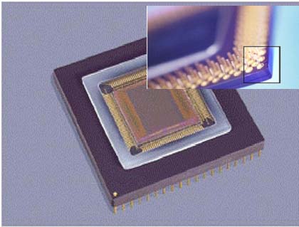 A CMOS image sensor. Courtesy nasa.gov.
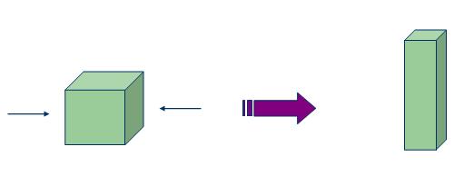 Decreasing the cross-sectional area of a pixel changes its geometry.
 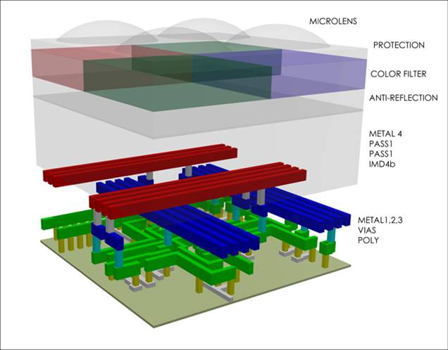 A pixel is not just a dot.